
ASIC Chips : How are ASIC chips designed for mining?
- Stellar Forge Mining

- Aug 15, 2023
- 2 min read
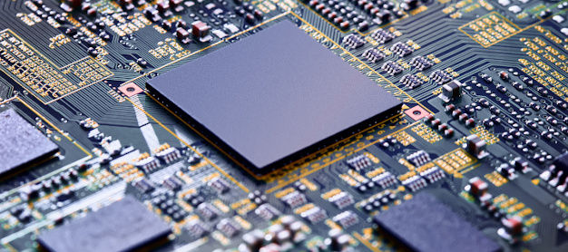
ASIC (Application-Specific Integrated Circuit) chips are custom-designed integrated circuits that are created to perform a specific function or set of functions. They are distinct from general-purpose microprocessors, such as those found in computers, because they are optimized for a particular application, which allows for greater efficiency and performance. The process of creating ASIC chips involves several stages, including design, fabrication, and testing. Here's an overview of how ASIC chips are made:
1. Design and Specification:
The process begins with the design and specification phase. This is where the functionality, performance requirements, and other specifications of the ASIC are determined. Designers work closely with the customer to understand the application's requirements and develop a detailed design specification.
2. Architectural Design:
In this phase, designers create a high-level architectural design of the ASIC. This includes defining the overall structure of the chip, the arrangement of logic blocks, memory elements, input/output interfaces, and any specialized circuits needed for the application.
3. Logic Design:
During this stage, the high-level architectural design is translated into a detailed logic design using hardware description languages (HDLs) like VHDL or Verilog. The logic design represents the behavior and functionality of the various components on the chip.
4. Verification and Simulation:
Before moving on to fabrication, the logic design undergoes rigorous verification and simulation. This step ensures that the design behaves as intended, catching and correcting errors before physical implementation. Simulation helps to identify potential timing issues, logic errors, and functional problems.
5. Physical Design:
The physical design phase involves converting the logical representation of the ASIC into a physical layout that can be manufactured. This includes tasks such as floor planning (arranging components on the chip), placement (positioning components), routing (connecting components), and ensuring proper signal integrity.
6. Mask Generation:
Once the physical design is complete, a set of masks is generated. Masks are high-precision templates used in the semiconductor fabrication process to define the patterns that will be etched onto the silicon wafers.
7. Fabrication (Manufacturing):
The masks are used in the photolithography process to transfer the circuit patterns onto silicon wafers. The fabrication process involves a series of steps, including deposition of various materials (such as silicon, metal, and insulators), photolithography, etching, doping, and layering. These steps create the intricate patterns and structures of the ASIC.
8. Packaging and Testing:
After fabrication, the individual chips are separated from the wafer and packaged into protective enclosures. The packaging provides electrical connections to the outside world and safeguards the chip from environmental factors. Following packaging, extensive testing is conducted to ensure that the ASIC functions correctly and meets the design specifications.
9. Finalization and Distribution:
Once the chips have been tested and verified, they are ready for distribution to customers or integration into larger systems. The ASIC chips are then used in various applications, ranging from consumer electronics to industrial and automotive systems.
It's important to note that ASIC design and manufacturing are complex processes that require specialized expertise, tools, and facilities. The specific steps and technologies involved can vary depending on the complexity of the design, the desired performance, and the semiconductor manufacturing technology used at the time.


